


Common Issues in Mobile Phone EMC Testing
With the widespread use of smartphones, electromagnetic compatibility (EMC) has become a key factor affecting user experience and product quality. From electrostatic interference to signal disturbances, mobile phones face multiple challenges in complex electromagnetic environments. This article analyzes typical issues in mobile phone emc testing based on real-world cases and offers targeted optimization solutions.
Test Scenarios and Core Issues
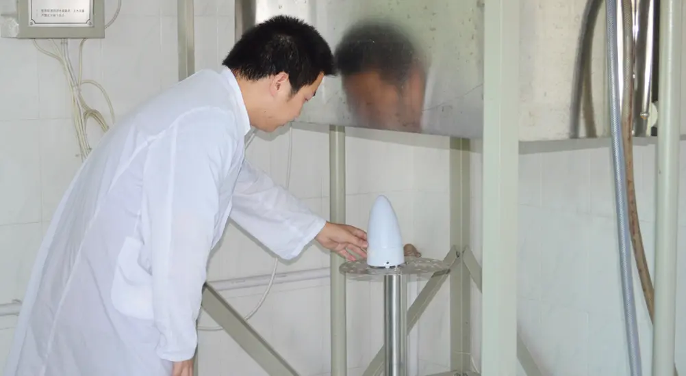
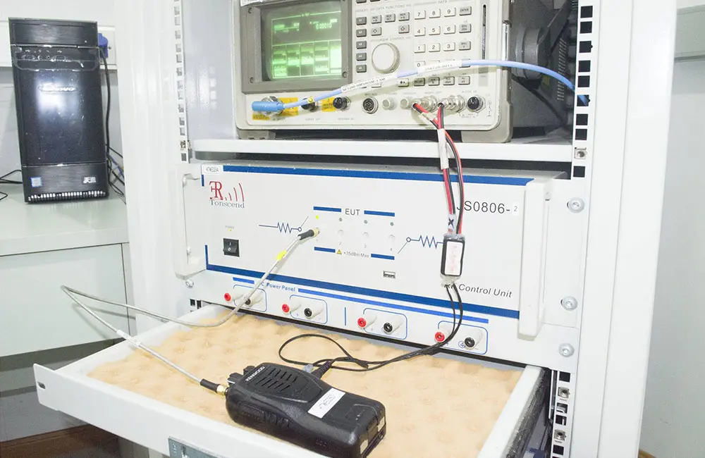
Electrostatic Discharge (ESD) Immunity Test
ESD is one of the most common sources of electromagnetic interference in daily life. Typical issues encountered during testing include:
- Call Interruptions: When electrostatic pulses couple into the RF circuit, it causes a sudden drop in signal-to-noise ratio. For example, in a ±8kV contact discharge test, one model experienced 3-second intermittent audio due to insufficient redundancy in the ESD protection circuit of the RF front-end chip.
- System Malfunctions: The baseband reset circuit can be sensitive to static electricity. One model frequently rebooted during ±15kV air discharge testing, which was traced to improper selection of the filtering capacitor on the reset pin.
- Hardware Damage: In extreme cases, static discharge up to 20kV may cause permanent damage to components. In one case, the power management chip suffered insulation breakdown due to ESD, rendering the entire device unable to power on.
Electrical Fast Transient/Burst (EFT/B) Immunity Test
The high frequency and energy of EFT/B pose serious challenges to internal phone circuits:
- Communication Link Failures: Bursts coupled through power lines rapidly charge semiconductor junction capacitance, leading to bit errors on SPI buses between baseband and RF modules. A 4G model lost LTE signal during a 4kV EFT/B test.
- Software Logic Disruption: The MCU may misinterpret pulse interference as control signals, causing touch failures or app crashes. In one test, interference was mistakenly recognized as a volume control command.
- Functional Module Failure: Sustained pulse interference can cause bit flipping in memory chips. One model's EMMC chip lost user data after testing due to chip-select signal coupling interference.
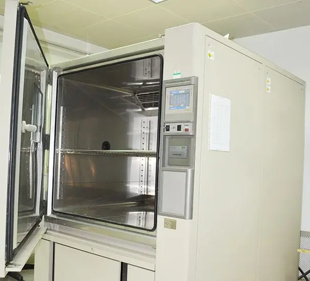
Radiated and Conducted Emissions Testing
Radiated Emissions (RE) and Conducted Emissions (CE) exceeding limits are common non-compliance issues in EMC certification:
- Charger Compatibility: Third-party chargers lacking EMC design may become interference sources. One brand showed CE levels exceeding CISPR 32 limits by 6dBμV in the 150kHz–30MHz range when using a non-original charger.
- System-Level Coupling: When the phone and charger operate together, RF and power circuits may create coupling interference. In a 5G model, RE exceeded limits at the 2.4GHz band due to a ground loop formed between the PA module and power converter.
Improvement Recommendations
01. Design Stage
PCB Layout and Grounding
- Use multilayer boards with tightly coupled power and ground planes to reduce power plane impedance.
- Physically isolate RF circuits from digital circuits to avoid crosstalk (e.g., maintain a minimum 5mm distance between the RF antenna and CPU).
- Add shielding loops to critical signals (clock, reset lines) to reduce ESD coupling risk.
Component Selection and Filtering
- Select chips with ESD protection levels ≥±15kV (HBM), such as baseband chips with built-in ESD clamps.
- Add ferrite bead + capacitor filter networks at power inputs (e.g., 100nF capacitor + 100Ω/100MHz bead) to suppress EFT/B pulses.
- Chargers must comply with GB 4943.1 standards and include common-mode chokes and X/Y capacitors to reduce conducted emissions.
Shielding and Structural Design
- Use multi-point grounding for the metal mid-frame and control gaps under 0.1mm to suppress radiated leakage.
- Add conductive fabric pads at camera and speaker openings to form a complete Faraday cage structure.
02. Production Stage
Component Screening: Perform batch sampling on sensitive components (e.g., RF switches, oscillators) to ensure ESD and EFT/B performance consistency.
Soldering Process Optimization: Use nitrogen reflow soldering to reduce PCB carbonization and avoid emissions due to poor grounding.
Final EMC Screening: Add quick EMC inspection equipment at the end of the production line to conduct 100% sampling for ESD and EFT/B immunity.
Future Trends
With the advancement of 5G-A and 6G technologies, mobile frequencies are expanding to millimeter-wave bands (e.g., 28GHz, 39GHz), presenting new emc testing challenges:
- High-Frequency Radiation Control: Near-field radiation from mmWave antenna arrays requires more precise simulation and testing methods.
- Multi-Antenna Coupling: Massive MIMO may induce antenna-to-antenna mutual coupling effects, requiring novel decoupling structures.
- Power Efficiency vs EMC Balance: Higher power consumption of high-frequency components leads to thermal-electromagnetic coupling issues, necessitating co-design of thermal and EMC considerations.
JJR Laboratory in China provides professional testing services.
Email:hello@jjrlab.com
Write your message here and send it to us
 Where to Get German LFGB Testing Done?
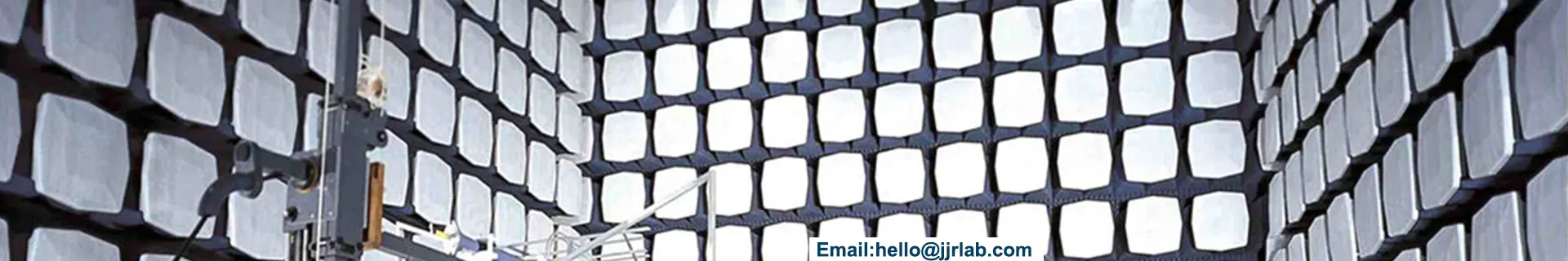
 966 Fully Anechoic Chamber
 Power Adapter UL1310 Certification
 Standard for Air Conditioners and Dehumidifiers: I
 Guide to Children's Product Safety and Compliance
 US Mattress Compliance Certification
 Canadian Site Mattress Compliance Testing
 Compliance for US Lithium-Battery-Powered Househol
Leave us a message
24-hour online customer service at any time to respond, so that you worry!