


What is the meaning of EMC?
EMC
English Name: Electro Magnetic Compatibility
Refers to the ability of electronic products or electrical equipment to operate normally according to design requirements in a specified electromagnetic environment.
")
EMC = EMI + EMS
EMI: Electromagnetic Interference refers to the electromagnetic energy that should not exceed the specified standards when electronic products are operating normally. The test items and corresponding standards vary depending on product functions, form, and application scenarios.
Basic emi test Items:
① Power line conducted emissions (CE) testing (fcc 450KHz-30MHz, CISPR 22 150KHz-30MHz)
② Signal conducted emissions (CE) testing (FCC 450KHz-30MHz, CISPR 22 150KHz-30MHz)
③ Radiated emissions (RE) testing (30MHz-1GHz)
④ Harmonic current testing (FCC part15:1GHz-18GHz, EN300 328:1GHz-12.75GHz)
⑤ Voltage fluctuation and flicker testing
Classification:
EMI is generally classified into two levels: Class A(industrial grade) & Class B(consumer grade).
For example, in a 3m radiation test:
Class A: 30-230MHz, max 50dBuV
Class A: 230-1000MHz, max 57dBuV
Class B: 30-230MHz, max 40dBuV
Class B: 230-1000MHz, max 47dBuV
EMS: ElectroMagnetic Susceptibility refers to the ability of electronic products to operate normally when subjected to electromagnetic interference within the specified standard range in a given environment. The test items and corresponding standards vary based on product functions, form, and application scenarios.
Basic EMS Test Items:
① Electrostatic Discharge (ESD)
② Electrical Fast Transient/Burst (EFT)
③ Surge
④ Radiated Susceptibility (RS)
⑤ Conducted Susceptibility (CS)
⑥ Voltage Dips and Interruptions (DIP)
Classification:
EMS is classified into Class A\~Dbased on the operational state of the product after interference is applied.
For example, in electrostatic testing:
① Class A: The device continues to operate normally after or during testing.
② Class B: The device may restart during or after the test but can return to normal operation without human intervention.
③ Class C: The device may freeze (or other abnormal phenomena) during or after the test but can restart and function normally after manual adjustments.
④ Class D: The device is damaged and cannot be restarted despite adjustments.
Strictness Level:
EMI: B > A
EMS: A > B > C > D
International Standards:
① International Electrotechnical Commission (IEC)
② International Organization for Standardization (ISO)
③ Institute of Electrical and Electronics Engineers (IEEE)
④ European Telecommunications Standards Institute (ETSI)
⑤ International Radio Consultative Committee (CCIR)
⑥ International Telecommunication Union (ITU)
⑦ IEC has various subcommittees for EMC standard research
Product Safety and EMC Certification Organizations in Various Countries:
① China: CCC
② Taiwan: CE
③ Europe: CE
④ Japan: VCCI
⑤ South Korea: MIC
⑥ USA: FCC
⑦ Canada: ICES
⑧ Australia: C-Tick
EMC Design Considerations:
Example of AC/DC switch power supply conduction rectification:
① Conducted emissions between 150KHz-1MHz are dominated by differential mode interference. Between 1MHz-5MHz, both differential and common mode interferences are involved, and above 5MHz, common mode interference dominates.
② Increasing the X capacitor appropriately can optimize the total over-standard issue near the 150KHz frequency point.
③ If over-standard below 1MHz, increase the inductance of the single-winding inductor in the PFC input section.
④ Around 200KHz, spikes are primarily caused by leakage inductance.
⑤ Adding a resistor of several KΩ to tens of KΩ in parallel with the common mode inductor helps address the 150KHz-1MHz frequency point.
⑥ Asymmetry in the inductance of the common mode inductor can cause conduction interference beyond 150KHz-3MHz.
⑦ Noise from circuit switches primarily occurs around 20MHz.
⑧ During PCB design, transformers and common mode inductors should be spaced to avoid mutual interference.
⑨ For three-wire input power designs, reduce Y-capacitor values from 2.2nF to 471.
⑩ For two-stage filters, removing the second-stage 0.22µF X capacitor may prevent oscillation between front and rear X capacitors.
11 Adding a pair of small differential mode inductors of several hundred µH before the common mode inductor.
12 For over-standard interference in the 1-5MHz range, adjust the X capacitance and add differential mode inductors to adjust the inductance.
13 For power supplies without Y capacitors, common mode interference under 1MHz is often severe.
14 Winding transformers with the same-name terminals on one side can reduce conduction interference from 1.0MHz to 5.0MHz.
15 For small power supplies, use two differential mode inductors. Reducing the turns of the differential mode inductors can lower conduction interference below 1MHz.
16 Increasing Y-capacitors can reduce common mode interference in the 1MHz-5MHz conduction range.
17 Placing small high-voltage surface-mounted capacitors in parallel with the input filter capacitor can lower conduction interference in the 1MHz-5MHz range.
18 Adding a shield winding to the transformer’s primary winding can reduce high-frequency interference by connecting one end to the power terminal and the other through a capacitor to ground.
19 Increasing the Y-capacitor value can reduce conduction interference, and changing transformer winding methods (such as adding more layers of tape) can improve this.
20 Increasing the transformer inductance can reduce conduction interference in a half-loaded state.
21 Using the secondary auxiliary winding to shield the primary winding can reduce conduction interference between 3MHz-15MHz.
22 Adding a small capacitor to the transformer’s input voltage pin can reduce conduction interference between 25MHz-30MHz.
23 Placing a 101 capacitor to ground at the MOSFET’s D pin can reduce conduction interference between 25MHz-30MHz.
24 For over-standard conduction at 25MHz, add a common mode inductor at the output end.
Example of AC/DC switch power supply radiation rectification:
① 30MHz-50MHz is generally caused by high-speed switching of MOSFETs, and 50MHz-100MHz is caused by reverse recovery current of output rectifier diodes. Radiation above these frequencies is generally very small and can usually meet standards.
② Using a slow diode like 1N4007 in the RCD snubber circuit can reduce radiation interference from 30MHz-50MHz.
③ Using a slow diode like 1N4007 in the VCC supply voltage can reduce radiation interference from 30MHz-50MHz.
④ Adding a small absorption capacitor to the MOSFET’s D pin can reduce radiation interference from 30MHz-50MHz.
⑤ Adding a small capacitor to the transformer’s input voltage pin can reduce radiation interference from 30MHz-50MHz.
⑥ When designing PCB Layout, try to minimize the circuit loop formed by large electrolytic capacitors, transformers, and MOSFETs.
⑦ Minimize the loop formed by the transformer, output diodes, and output smoothing electrolytic capacitors.
⑧ Adjusting the absorption circuit parameters of the output rectifier diodes can improve interference above 50MHz.
⑨ Changing the impedance of the Y-capacitor branch between the primary and secondary can help improve interference above 50MHz by adding a suitable resistor.
⑩ Adding shielding copper foil during transformer winding can suppress radiation into space.
Each design may differ due to factors such as PCB layout, selected materials, and the application environment. The problems encountered during testing and corresponding solutions may also vary. The above suggestions are for reference only.
Additionally, when rectifying EMC in switch power supplies, both conducted and radiated emissions must be considered. Measures to rectify conducted emissions may affect radiation and vice versa. Therefore, for the same frequency point exceeding standards, the solution is not unique and requires a plan that minimizes the impact on the entire system. After EMC rectification, it is crucial to ensure that key indicators like power efficiency, dynamic response, and load adjustment rate are not negatively affected.
Email:hello@jjrlab.com
Write your message here and send it to us
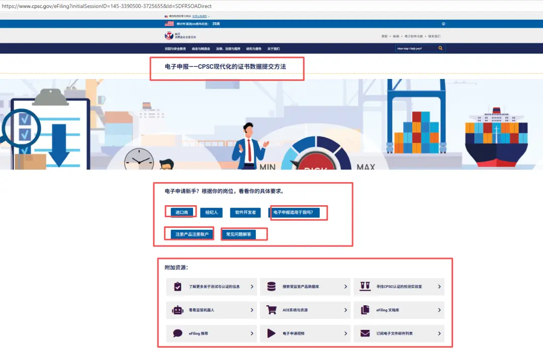 2026 US CPSC eFiling IOR Operation Guide
 CPSC eFiling Enforcement: IOR + Electronic Filing
The US eFiling Amazon and Temu Sellers Must Comple
CPSC eFiling Enforcement: IOR + Electronic Filing
The US eFiling Amazon and Temu Sellers Must Comple
 New US CPSC eFiling Regulations Guide
 CPSC eFiling Process Guide for Amazon Shipments
 SAA approval testing services
 US FCC 100% Hearing Aid Compatibility (HAC) for Mo
 Australia Food Contact Testing
Leave us a message
24-hour online customer service at any time to respond, so that you worry!